

Avalanche Photodiode or APDs are highly sensitive semiconductor appliances that have the potential to change optical signals into electrical signals. The high performance SI APDS are used in applications where detection of sensitive light is required. It is a type of photodiode that is used in a wide array of applications that other photodiodes are not able to initiate.
Some basics of avalanche photodiode
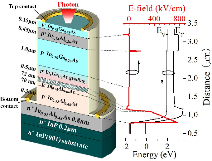
APD or Avalanche Photodiode features the same structure as PIN photodiode or PN. The primary distinction of avalanche photodiode with other photodiode forms is that APD functions under top reverse bis condition. This leads to the multiplication of electrons and holes as created by the impact of light/photon.
When light enters the depleted area, there is a creation of holes and an electron pair. They will be drawn by high electric fields away from one another. The velocity of the charged carriers will increase to an extent that they will clash with the lattice. This will further create holes and electron pairs and the process continues. This avalanche act aids the diode to increase several times and thereby offering a greater level of light or photon sensitivity.
Difference between Avalanche Photodiode and PIN Photodiode
The difference between the two are briefly mentioned below:
- Avalanche Photodiode has four layers. They are P+, I, P, and N+. On the other hand, PIN Photodiode includes three layers, like P+, I, and N+.
- The response time for Avalanche Photodiode is high, whereas, the response time for PIN Photodiode is low.
- The internal gain for Avalanche Photodiode is 200 Db. Whereas, the internal gain is insignificant for PIN Photodiode.
- Avalanche Photodiode is known to have a high reverse bias voltage. PIN Photodiode, on the other hand, has low reverse bias voltage.
- There is stability in high temperatures for Avalanche Photodiode. Furthermore, PIN Photodiode doesn’t have high-temperature stability.
- The output current for Avalanche Photodiode is low. For PIN Photodiode, the multiplication of carrier current leads to amplifier current value.
- Avalanche Photodiode has high noise, whereas, PIN Photodiode has low noise.
- The amplifier in Avalanche Photodiode is not necessary because of the available gain. On the other hand, the amplifier is necessary for PIN Photodiode because of not the available gain.
Circuit conditions of APDs
To function, APD or Avalanche Photodiode demands high reverse bias. When silicon is concerned, the reverse bias will range between 100 volts and 200 volts. Because of the high reverse bias level of high performance SI APDS, the gain effect is expected around 100 volts. For industrial purposes, there are APD or Avalanche Photodiodes that make use of specialized manufacturing processes and have access to as high bias voltage as 1500 volts. When such a high-level reverse bias voltage is in operation, the APD or Avalanche Photodiodes can rise to 1000 volts. This is particularly beneficial where photon sensitivity is of utmost importance. But this means that extra circuitry and safety aspects should be considered as high voltages are used.
Advantages of Avalanche Photodiode
Though there are several disadvantages of APDs, the advantages overpower the cons. Some of the primary advantages of APD or Avalanche Photodiode are as mentioned below:
- The sensitivity range is very high
- The response time is quick
- The performance is top-notch
- Easily identifies low-intensity light
- Produces a wide array of charge carrier pairs
Applications of Avalanche Photodiode
There is a plethora of applications and devices where high performance SI APDS are used. Some of the common applications are mentioned below:
- Laser microscopy
- PET scanner
- Laser scanner
- Laser rangefinders
- Speed gun
- Barcode reader
- Antenna analyzer bridge
- OFC (Optical Fiber Communication) receivers
- OTDR (Optical Time Domain Reflectometers
Conclusion
The breakdown of the avalanche takes place when the photodiode is under the highest reverse voltage. The high voltage increases the electric field beyond the depletion layer. When high-sensitive photon/light enters the “P+” layer, it gets absorbed within the “P” layer. This leads to the generation of electron pairs. When the velocity is at its highest, the charge carriers will clash and produce new electron-hole pairs and resulting in even higher photocurrent sensitivity. The high performance SI APDS is widely used in applications and devices where high-level photosensitivity is required. Its capacity to transform optical signals into electrical signals makes it widespread and popular in several industries around the world.